STMicroelectronics SGT350R70GTK E-Mode PowerGaN Transistor
STMicroelectronics SGT350R70GTK E-Mode PowerGaN Transistor is a high-performance enhancement-mode PowerGaN transistor optimized for efficient power conversion in demanding applications. With a drain-source voltage rating of 700V and a maximum on-resistance of 350mΩ, the STMicroelectronics SGT350R70GTK delivers low conduction losses and fast switching capabilities thanks to Gallium Nitride (GaN) technology. Packaged in a thermally enhanced DPAK format, the device supports high current handling and improved heat dissipation, suitable for high-density power designs. A low gate charge and output capacitance enable high-frequency operation, ideal for use in power factor correction (PFC), resonant converters, and other advanced power topologies in industrial, telecom, and consumer electronics sectors.Features
- Enhancement mode normally off transistor
- Very high switching speed
- High power management capability
- Extremely low capacitances
- Zero reverse recovery charge
- ESD safeguard
- RoHS compliant
Applications
- Consumer electronics
- Industrial systems
- Data centers
- Adapters for tablets, notebooks, and AIO
- USB Type-C® PD adapters and quick chargers
- Resonant converters
- Power Factor Correction (PFC) stages
Specifications
- 700V maximum drain-source voltage
- 800V maximum transient drain-source voltage at tp < 200μs
- -1.4V to 7V maximum gate-source voltage
- 6A maximum continuous drain current at +25°C
- 10A maximum pulse drain current at tp = 10μs
- 47W maximum total power dissipation at +25°C
- 2.6V typical source-drain reverse conduction voltage
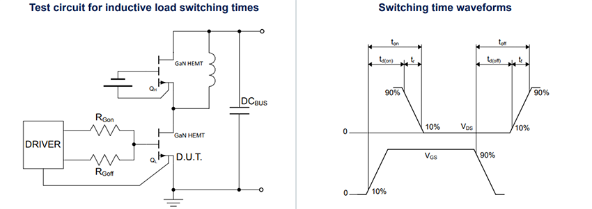
- Switching
- 0.9ns typical turn-on delay time
- 3.5ns typical rise time
- 1.2ns typical turn-off delay time
- 6.1ns typical fall time
- Static
- 12μA maximum drain-source leakage current
- 30μA typical gate-source leakage current
- 1.2V to 2.5V gate threshold voltage range
- 350mΩ maximum static drain-source on-resistance
- 2kV Human Body Model (HBM) ESD protection
- -55°C to +150°C operating junctin temperature range
- Dynamic
- 50pF typical input capacitance
- 15pF typical output capacitance
- 0.2pF typical reverse transfer capacitance
- 20pF typical equivalent output capacitance, energy related
- 28pF typical equivalent output capacitance, time related
- 11Ω typical intrinsic gate resistance
- 2.2V typical gate plateau voltage
- 1.5nC typical total gate charge
- 0.15nC typical gate-source charge
- 0.5nC typical gate-drain charge
- 0nC typical reverse recovery charge
- 13nC typical output charge
- Thermal resistance
- 2.63°C/W junction-to-case
- 56°C/W junction-to-ambient
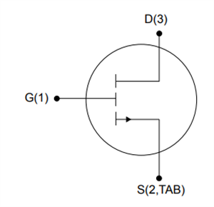
Schematic

Test Circuits

Publicado: 2025-10-20
| Actualizado: 2025-10-28


