


Lattice Semiconductor iCE40 UltraPlus FPGAs
Lattice Semiconductor iCE40 UltraPlus FPGAs are designed for ultra-low-power mobile applications, which include smartphones, tablets, and hand-held devices. The iCE40 UltraPlus family includes integrated SPI and I2C blocks to interface virtually with all mobile sensors and application processors. These iCE40 FPGAs feature device density of 2800 to 5280 range Look Up Tables (LUTs) with programmable I/Os, which can be used as either SPI/I2C interface ports or general-purpose I/Os. The iCE40UP is available in very small form factor packages, as small as 2.15mm x 2.55mm, which allows the device to fit into many applications easily.
The Lattice iCE40UP5K FPGAs feature 30 embedded block RAM memory blocks, 120 embedded block RAM memory bits, on-chip oscillators, and 8 DSP blocks. Whereas icE40UP3K FPGAs feature 20 embedded block RAM memory blocks, 80 embedded block RAM memory bits, on-chip oscillators, and 4 DSP blocks. Typical applications include iCE40 ultra devices, service LED, GPIO expander, Serial Data Input Output (SDIO) level shifter, and voice recognition for mobile applications.
Features
- Device logic architectures
- 5280 for iCE40UP5K FPGAs
- 2800 for iCE40UP3K FPGAs
- 40nm low-power processors
- 100µA standby current
- 1024kb single-port SRAM
- Two I/O pins to support I3C interface
- Two hardened SPI interfaces
- 24mA current drive RGB LED outputs
- 2.15mm x 2.55mm ultra-small form factor
- On-chip DSP
- WLCS and QFN packages
Applications
- Voice recognition applications
- Smartphones
- Tablets and consumer handheld devices
- Handheld commercial and industrial devices
- Multi-sensor management applications
- Sensor pre-processing and sensor fusion
- Sensor applications
- USB 3.1 Type C cable detect/power delivery applications
Additional Resource
Associated Tools
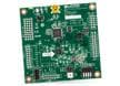
Lattice Semiconductor iCE40 UltraPlus Breakout Board
Rapid prototyping of user functions, effortless connectivity, and simple programming.
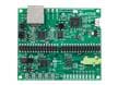
Lattice Semiconductor ICE40UP5KSWAEVN SWA Evaluation Board
Customizable and reduces cable and connector size while increasing reliability.
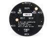
Lattice Semiconductor iCE40 UltraPlus 8:1 Microphone Aggregator Board
Daughter Board for iCE40 UltraPlus Mobile Development Platform for aggregation of up to 8 PDM mics.
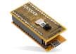
Lattice Semiconductor Himax HM01B0 UPduino Shield
Consists of UPdiono v2.0 and Himax HM01B0 adaptor board and is based on iCE40™ UltraPlus FPGA.
Associated Products
Lattice Semiconductor iCE40 Series MobileFPGA Family
Includes ultra-low power devices with flexible logic architecture.
Associated Software

Lattice Semiconductor Radiant Software
A full featured FPGA design tool suite that’s simple to use and is optimized for edge applications.